High‑end semiconductors have become indispensable in everyday life—often in ways we don’t notice. From personal consumer electronics and smart mobility to home automation, public infrastructure, healthcare, and entertainment, advanced chips are the silent enablers of modern convenience.
At the heart of this ecosystem lies thick‑film screen printing, a core manufacturing process for chip packaging and substrate production. Screen printers are not merely auxiliary tools; they are tightly coupled with the performance of premium devices. The precision of the printing equipment directly determines the upper limits of critical components in high‑reliability chips, making it one of the key enablers of advanced semiconductor manufacturing.

Image source: Internet
1. Critical Process Requirements for High‑End Chips
To meet the stringent demands of advanced packaging, thick‑film printers must excel in four key areas:
- Alignment Accuracy – In typical packaging environments, alignment precision must reach ±2 µm to ±5 µm. This ensures that multilayer patterns are perfectly superimposed, eliminating misregistration that can cause chip failure.
- Repetitive Printing Precision – Consistent reproduction within ±2 µm is essential for high‑volume production, especially for wafer‑level packaging and multilayer internal electrodes in components like MLCCs.
- Film Thickness Uniformity – Overall thickness variation across the entire print area should be ≤ ±3%. Uniform deposition of metallic pastes and dielectric layers is critical for subsequent sintering and wire bonding processes.
- Substrate Compatibility – The equipment must support 6‑inch, 8‑inch, and 12‑inch wafers, as well as various ceramic substrate sizes, covering the full range of current mainstream high‑end chip dimensions.
2. Mainstream Equipment Models for High‑End Chip Manufacturing
- 4‑Camera CCD Auto‑Alignment Thick‑Film Printer
This model features a four‑camera vision alignment system that significantly improves both throughput and accuracy. The print head angle and squeegee pressure are digitally adjustable, making it suitable for wafer‑level glass‑paste bonding and ceramic package printing. An integrated static‑elimination function protects sensitive chip components from electrostatic damage.
- JY‑HG‑250‑LTCC High‑Precision Four‑Post Printer
Designed specifically for LTCC, MLCC, and other chip‑supporting passive components, this printer offers a maximum print area of 250 × 250 mm. It holds one invention patent and five utility‑model patents. The machine reliably performs high‑precision internal electrode printing on 6‑inch and 8‑inch green ceramic tapes, making it ideal for mass production of passive components used in high‑end chips.
3. Key Process Applications
High‑end chips represent a technological barrier in the semiconductor industry, and their mass production heavily relies on high‑precision screen printing:
- Electrode Formation – High‑accuracy screen printing creates multilayer interconnects on ceramic substrates, providing reliable packaging carriers for power chips and RF chips, capable of handling high currents and efficient heat dissipation.
- Film Thickness Control – Precise uniformity of sensing and conductive layers prevents signal deviations, ensuring data integrity in advanced devices.
- Substrate Adaptation – The printing process is compatible with silicon‑based materials, yielding strong adhesion and good flexibility for long‑term reliability.
Screen printing offers both high compatibility and precision, establishing itself as the mainstream choice for high‑volume chip production—and the primary carrier for thick‑film processes in semiconductor packaging.
Recommended Equipment: JY‑HG‑250‑LTCC
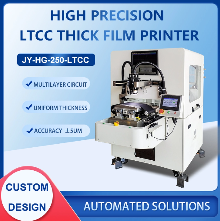
Maximum printing area: 250 × 250 mm.
Compatible substrates: 6″ or 8″ green ceramic tapes, ceramic substrates, electronic components, PCBs.
Patents: 1 invention patent, 5 utility‑model patents.
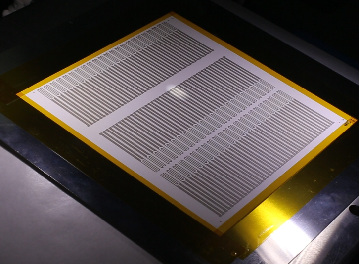
Printed Product Samples.
4. Conclusion
At JYUTEC Network Printing, we leverage our core thick‑film screen printing expertise to deliver highly adaptable, precision‑engineered solutions for advanced chip packaging. We are committed to meeting the ever‑tighter process requirements of semiconductor packaging, helping our customers improve product performance, yield, and consistency. Through deep customization and process optimisation, our equipment ensures stable, reliable mass production in critical applications, providing solid technological support to the global electronics supply chain. With a dedicated focus on precision engineering, we continue to drive the packaging industry toward higher accuracy and greater efficiency.