
 Finished functional ceramic metallization product printed using JYUTEC equipment
Surface metallization of functional ceramics is a process in which a metal layer is deposited or applied to a ceramic surface to improve its electrical conductivity, thermal conductivity, or other functional properties. Several methods can be used for this purpose, including electroless plating, direct copper bonding, thick-film metallization, and thin film metallization.
Thick film metallization, in particular, is a process that uses a high precision thick film screen printing machine to apply metal paste to the surface of functional ceramics. The printed layer is then subjected to high-temperature firing to form a metallized ceramic substrate.
The typical screen printing process involves preparing a screen based on the product design, preparing the appropriate paste, screen printing, drying, and high-temperature firing. The pastes used are primarily metal-based conductive pastes, including gold, silver, copper, and molybdenum-manganese (Mo-Mn) pastes, along with other electronic pastes.
Thanks to its well-established processing technology, uniform film thickness, relatively low cost, and suitability for automation, thick-film metallization is widely used to form metallization layers, conductive features such as circuit traces, and resistive layers on functional ceramic substrates.
In the following sections, we will explore the key application areas of thick-film metallization.
2.Power Electronics Applications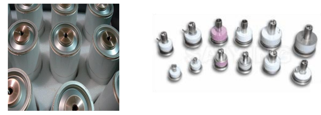
Ceramic Vacuum Interrupter (Image Source: Online)
Power electronics is a field focused on the use of electronic devices and systems to convert, control, and manage electrical power. Ceramic vacuum interrupters are key components in this field. By utilizing the excellent dielectric properties of the vacuum inside the sealed ceramic envelope, they rapidly extinguish arcs when the contacts separate, enabling safe circuit interruption and helping maintain stable power grid operation while reducing the risk of faults and accidents.
The JYUTEC IC-340B high-precision screen printer shown below is suitable for printing ceramic envelopes for vacuum interrupters. It offers a maximum printing area of 340 × 340 mm and supports customized fixtures, allowing multiple ceramic envelopes to be printed in a single cycle. By changing the fixture, the machine can also accommodate other products, meeting the needs of batch production across a variety of product types.
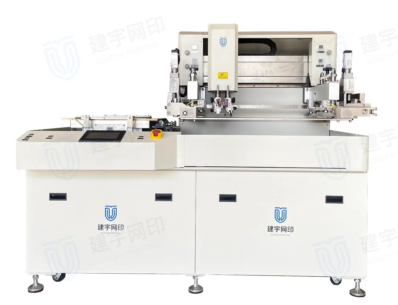
JYUTEC IC-340B Screen Printer
Featuring a left-right shuttle-table configuration and a motor-driven printing system, the IC-340B delivers consistent, uniform printing pressure and printing accuracy of ±5 μm. With its flexible configuration and strong expandability, the machine can be readily integrated into an automated production line tailored to the customer's manufacturing requirements.
3.Electric Vehicle (EV) Applications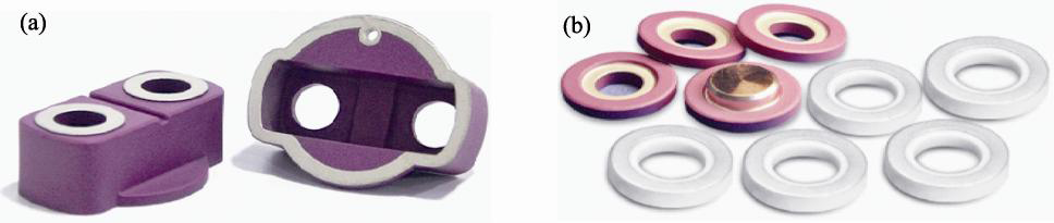
Image sources: Online — (a) Ceramic Relay; (b) Ceramic Sealing Ring
With the rapid growth of the electric vehicle industry in recent years, ceramic materials have become increasingly important in automotive applications. Ceramic components such as ceramic relays and ceramic sealing rings play important roles in these vehicles.
Ceramic relays are among the most widely used automotive electronic components, second only to electronic sensors in terms of application frequency. They are widely used in vehicle systems for starting, air conditioning, lighting, fuel pump control, communications, power windows, airbags, instrument panels, and fault diagnosis.
The screen printing processes for ceramic relays and ceramic sealing rings are broadly similar. A metal layer is printed onto designated areas of the ceramic surface for subsequent joining, typically using molybdenum-manganese (Mo-Mn) paste.
The JYUTEC IC-340B screen printer, also suitable for ceramic vacuum interrupter applications, can be adapted to these products simply by changing the product fixture and screen design. The printed layer thickness can also be adjusted by optimizing the screen printing process to meet specific product requirements.
JYUTEC IC-340B Screen Printer
An insulated-gate bipolar transistor (IGBT) is a power semiconductor device that combines the operating principles of a metal-oxide-semiconductor field-effect transistor (MOSFET) and a bipolar junction transistor (BJT). Ceramic substrates are widely used in IGBT modules due to their excellent thermal management performance and current-carrying capability.
Common ceramic substrate technologies include HTCC (High-Temperature Co-fired Ceramic), LTCC (Low-Temperature Co-fired Ceramic), DBC (Direct Bonded Copper), DPC (Direct Plated Copper), and AMB (Active Metal Brazing). Among these, LTCC, HTCC, and AMB substrates commonly use thick-film screen printing technology for metallization. Gold and silver pastes are typically used for LTCC and HTCC ceramic substrates, while specialized active brazing pastes are used in AMB substrate processing.
The JYUTEC HG-250-LTCC high-precision screen printer shown below is suitable for printing LTCC and HTCC ceramic substrates, as well as AMB substrates. It offers a maximum printing area of 230 × 230 mm and features a CCD-based automatic alignment system for high-precision printing, with an accuracy of ±5 μm.
A transparent enclosure above the printing head provides clear visibility while helping protect the printing area from dust and moisture loss, creating a favorable environment for the printing process. Depending on process requirements, the machine also supports multiple printing passes, with up to five repeat prints and a registration accuracy of ±5 μm.
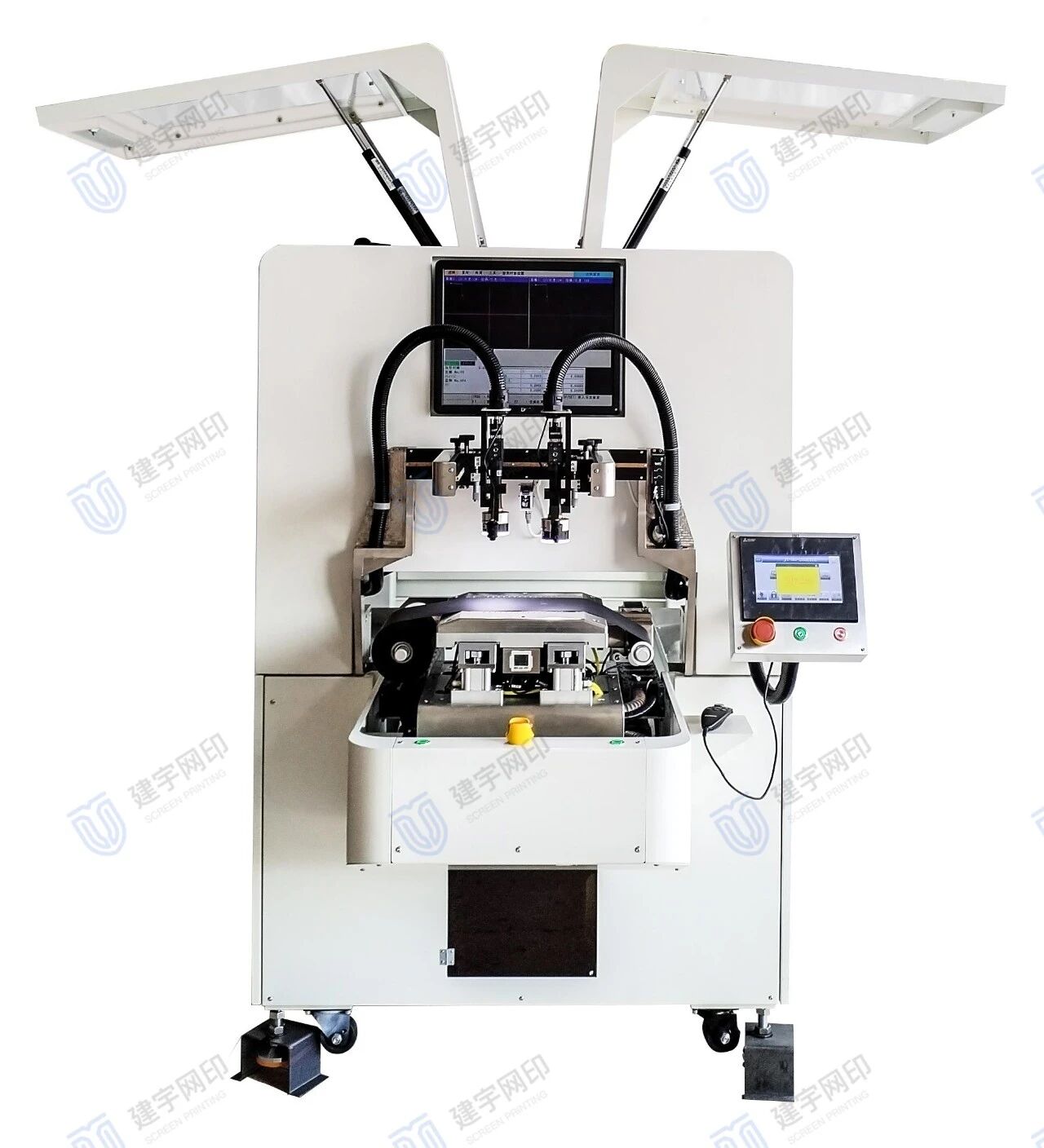
JYUTEC HG-250-LTCC Screen Printer
In the RF and microwave fields, ceramic dielectric filters are essential RF components in mobile communications. They filter transmitted and received signals by selectively allowing signals within specific frequency ranges to pass while attenuating unwanted frequencies, helping maintain signal integrity and communication accuracy.
The manufacturing process is complex and typically involves powder preparation, pressing and forming, sintering, grinding, metallization, assembly, and tuning. Metallization is a critical stage in ceramic dielectric filter manufacturing and accounts for approximately 35% of the overall process.
The JYUTEC IC-200A-CCD high-precision screen printer shown below is suitable for printing ceramic dielectric filters. It offers a maximum printing area of 200 × 200 mm and features a CCD-based automatic alignment system with a registration accuracy of ±5 μm. The machine is equipped with a porous ceramic worktable and an independent three-axis fine-adjustment mechanism for X, Y, and θ, making operation simple and convenient. It also achieves a film-thickness deviation of ±4 μm. JYUTEC IC-200A-CCD Screen Printer
As technology continues to advance, the combination of functional ceramics and metals will unlock greater potential across an expanding range of applications. As a key process connecting functional ceramics with metallic materials, thick-film metallization printing will continue to play an important role in power electronics, new energy vehicles, IGBT modules, and RF and microwave communications.
Looking ahead, we expect continued innovation and development in the thick-film screen printing industry, bringing higher-precision equipment and more comprehensive screen printing solutions for functional ceramic metallization. These advancements will help create new possibilities for modern industrial manufacturing.


